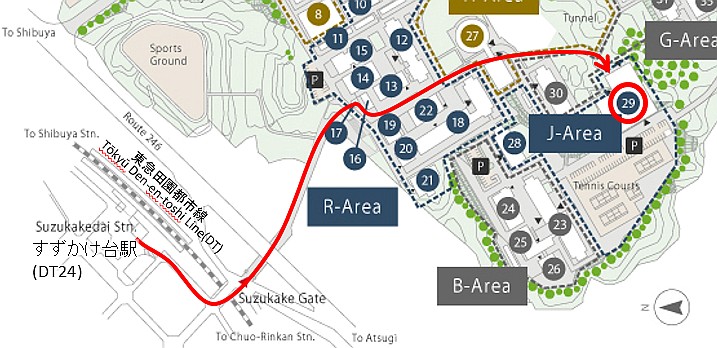
Suzukakedai map
(#29 in J area in the above link)
Tokyo Institute of Technology,
School of Materials and Chemical Technology
Department of Materials Science and Engineering
J2-49, Bld.J2, Room 1502,
4259 Nagatsuta, Midoriku, Yokohama, Kanagawa, 226-8503 Japan
TEL&FAX:+81(0)45-924-5674
Email:
sannomiya.t.aa (at) m.titech.ac.jp

Research
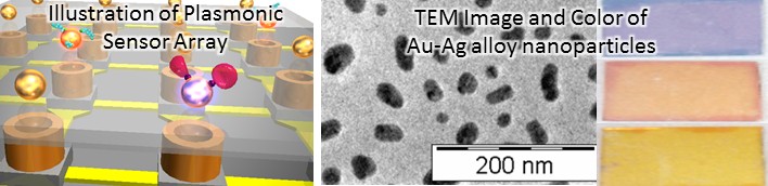
Functional Plasmonic Materials
- highly efficient, sensitive and fast optical devices -
With nanostructured optical materials, it is possible to focus the light energy into nanoscale dimensions far beyond the diffraction limit of light. One way of doing this is to use plasmonic materials, where oscillation of free electrons in metallic materials, so called "plasmon", causes resonances in a nanoscopically confined space. Since the plasmonic resonance is extremely sensitive to the surface permittivity change and can confined the light energy in a small space, highly efficient light energy harvesting/conversion, fast and effcient light emission, optical circuit, or super sensitive portable sensing would be possible. Such technology would realize fast communication, energy-efficient portable devices, sensitive pollutanct detection in the field, medical diagnostics at home etc. In our group, we cleverly combine self-assembly and lithographic technique to control the confinement of free electrons to tune the plasmonic resonance for new type of plasmonic sensing devices. We are also good at controlling the combosition, crystallinity, electron energy and mesoscopic structure of such materials. We have various national and international collaborations such as ETH Zurich, Chalmers Univ. Tech., ICFO, Weizmann Inst., Kobe Univ, Kyushu Univ., etc.
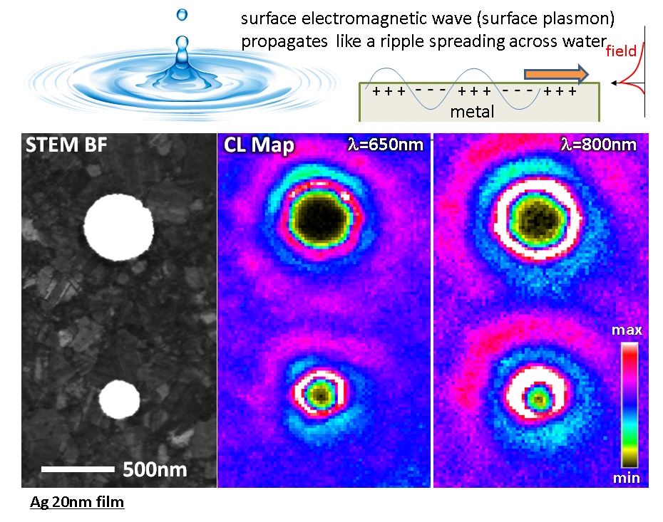
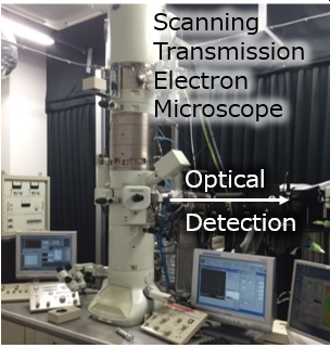
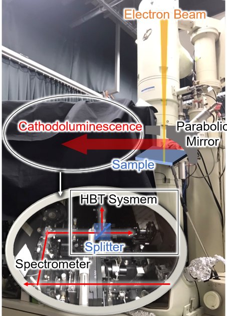
Visualization of Surface Plasmons
- Cathodoluminescence Scanning Transmission Electron Microscopy -
Confined light field in nanoplasmonic structures is not accessible by ordinary techniques based on light. We observe surface plasmons excited by accelerated electron beam. This technique (cathodoluminescence) enables visualization of the light field with 1 nm spatial resolution in combination with aberration corrected scanning transmission electron microscopy (STEM). Spectro-scopic mapping of the emitted light gives us real space light field distribution at different wavelengths.
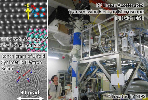
Development of Transmission Electron Microscopy Techniques
- Create "Eyes" for Material Research -
Transmision electron microscopy (TEM) with atomic resolution is an indispensable tool to develop new materials. Since its appearance in the early 20th century, it is still evolving. We are developing new TEM-based techniques and applications, as well as new STEM-CL methods. Such new "eyes" discover new materials and create new science.
We have collaborations related to this research with National Inst. Physiological Sci. as well as industries, such as Terabase Inc., and JEOL Ltd.
For details, go to Publication List
- highly efficient, sensitive and fast optical devices -
With nanostructured optical materials, it is possible to focus the light energy into nanoscale dimensions far beyond the diffraction limit of light. One way of doing this is to use plasmonic materials, where oscillation of free electrons in metallic materials, so called "plasmon", causes resonances in a nanoscopically confined space. Since the plasmonic resonance is extremely sensitive to the surface permittivity change and can confined the light energy in a small space, highly efficient light energy harvesting/conversion, fast and effcient light emission, optical circuit, or super sensitive portable sensing would be possible. Such technology would realize fast communication, energy-efficient portable devices, sensitive pollutanct detection in the field, medical diagnostics at home etc. In our group, we cleverly combine self-assembly and lithographic technique to control the confinement of free electrons to tune the plasmonic resonance for new type of plasmonic sensing devices. We are also good at controlling the combosition, crystallinity, electron energy and mesoscopic structure of such materials. We have various national and international collaborations such as ETH Zurich, Chalmers Univ. Tech., ICFO, Weizmann Inst., Kobe Univ, Kyushu Univ., etc.
Visualization of Surface Plasmons
- Cathodoluminescence Scanning Transmission Electron Microscopy -
Confined light field in nanoplasmonic structures is not accessible by ordinary techniques based on light. We observe surface plasmons excited by accelerated electron beam. This technique (cathodoluminescence) enables visualization of the light field with 1 nm spatial resolution in combination with aberration corrected scanning transmission electron microscopy (STEM). Spectro-scopic mapping of the emitted light gives us real space light field distribution at different wavelengths.
Development of Transmission Electron Microscopy Techniques
- Create "Eyes" for Material Research -
Transmision electron microscopy (TEM) with atomic resolution is an indispensable tool to develop new materials. Since its appearance in the early 20th century, it is still evolving. We are developing new TEM-based techniques and applications, as well as new STEM-CL methods. Such new "eyes" discover new materials and create new science.
We have collaborations related to this research with National Inst. Physiological Sci. as well as industries, such as Terabase Inc., and JEOL Ltd.
For details, go to Publication List
Instrument
Transmission Electron Microscope(TEM) / Scanning Transmission Electron Microscope(STEM)
Cathodoluminescence STEM, CFEG Aberration Corrected TEM / STEM R005
 Film Deposition
Physical Vapor Deposition (Sputtering, Arc/Themal Evaporation)
Optical Instrument
Vis-NIR Spectrometer, Spectro-microscope, Fluorescent Microscope, Temperature Variable Vacuum Spectrometer
Surface Characterization
Atomic Force Microscope (AFM), Scanning Electron Microscope (SEM) with high/low vac modes
Surface Modification
Plasma Cleaner, UV Ozone Cleaner, Wet Chemistry Facilities
We also use shared instrument : Atomic Force Microscope (AFM), Scanning Electron Miscroscope(SEM), Vibrating Sample Magnetometer(VSM) etc.
Simulation & Software Development
Electromagnetics (Optics) : Finite Element Method (FEM), Multiple Multipole Program(MMP), Boundary Element Method (BEM), Finite Difference Time Domain (FDTD)
Ab-initio Calculation : Materials Studio (CASTEP)
Various Self-coded Softwares (Matlab, C++, VB, Mathematica, Python etc)
Cathodoluminescence STEM, CFEG Aberration Corrected TEM / STEM R005
Film Deposition
Physical Vapor Deposition (Sputtering, Arc/Themal Evaporation)
Optical Instrument
Vis-NIR Spectrometer, Spectro-microscope, Fluorescent Microscope, Temperature Variable Vacuum Spectrometer
Surface Characterization
Atomic Force Microscope (AFM), Scanning Electron Microscope (SEM) with high/low vac modes
Surface Modification
Plasma Cleaner, UV Ozone Cleaner, Wet Chemistry Facilities
We also use shared instrument : Atomic Force Microscope (AFM), Scanning Electron Miscroscope(SEM), Vibrating Sample Magnetometer(VSM) etc.
Simulation & Software Development
Electromagnetics (Optics) : Finite Element Method (FEM), Multiple Multipole Program(MMP), Boundary Element Method (BEM), Finite Difference Time Domain (FDTD)
Ab-initio Calculation : Materials Studio (CASTEP)
Various Self-coded Softwares (Matlab, C++, VB, Mathematica, Python etc)